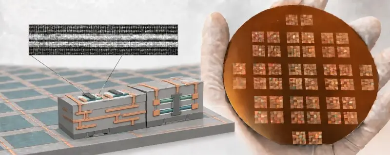
Harnessing Oxygen to Direct Crystal Formation
Researchers in South Korea have developed a breakthrough technique to precisely control the growth of two-dimensional semiconductors. By introducing oxygen during the manufacturing process, the team successfully prevents crystals from forming in unintended locations. This advancement marks a critical step toward integrating these high-performance materials into commercial computer chips by 2030.
Latest news
 Anthropic Unveils Claude Duet For Background AI Tasks
 Eiliko Creator Hires Independent Security Firm After Flawy Robot Charm Exposed
 Musk Compares Optimus Robot Training to Raising a Toddler
 Atari VCS Software Store Closes in February 2027
Current semiconductor manufacturing struggles with the structural uniformity of 2D materials. These ultra-thin layers are essential for creating faster, more energy-efficient processors. However, erratic crystal growth often leads to defects that render the materials unusable for industrial-scale production. The new method offers a reliable way to ensure consistent quality across large surfaces.
The research team discovered that oxygen acts as a stabilizing agent during the chemical vapor deposition process. By carefully regulating oxygen levels, scientists can inhibit the nucleation of crystals in unwanted areas. This ensures that the semiconductor layers grow in a perfect, continuous lattice structure.
Can This Technology Replace Traditional Silicon?
Previous attempts to refine these materials often resulted in fragmented or damaged layers. This new approach maintains the integrity of the 2D sheets while significantly reducing waste. It provides a scalable pathway for manufacturers to adopt these materials without overhauling existing fabrication infrastructure.
The industry has long sought to move beyond traditional silicon to meet the demands of modern computing. 2D semiconductors offer superior electrical properties, which could lead to devices that are significantly smaller and faster. While silicon remains the standard, this development brings 2D materials closer to practical, real-world application.
Frequently Asked Questions
Widespread adoption could revolutionize everything from mobile devices to high-end data centers. If the team meets their goal for commercialization by 2030, the technology will likely define the next decade of hardware engineering. It represents a major leap toward overcoming the physical limitations of current chip architectures.
Why is oxygen used in this process? Oxygen is used to suppress the formation of crystals in incorrect locations during the growth phase. This allows for a more uniform and defect-free semiconductor layer.
When will this technology be ready for commercial use? The research team is aiming for commercial integration by 2030. This timeline depends on successfully scaling the process for mass manufacturing environments.
Comments
Leave a comment